Ultrafast pulse generation, filtering, and modulation
Distributed Waveform Generator
Sub-nanosecond pulse generation is a critical function in radar, instrumentation, and most recently, UWB impulse-radios (IR-UWB)[1]. The challenge in its circuit implementation is not only to achieve the large signal bandwidth, but also to accomplish this with low power consumption and small circuit complexity (i.e. low cost). The latter two requirements are usually related, and are particularly important for battery-powered IR-UWB systems such as wireless sensor networks. Built-in modulation capability is also highly desirable for such a pulse generator since it can simplify the transceiver architecture, and hence lower power consumption and cost. In order to accommodate process variations, regulatory difference, changes in channel environment and antenna characteristics, an IR-UWB pulse generator also needs to be reconfigurable for different pulse shapes and spectra. In this paper, we present a distributed waveform generator (DWG)[2] circuit in a time-interleaved architecture suitable for standard CMOS implementation. It can directly synthesize waveforms in sub-nanosecond regime with reconfigurable spectra and built-in on-off keying modulation capability for IR-UWB communications.
Distributed Waveform Generator Architecture
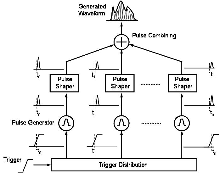
Fig.1 shows the generic architecture of proposed distributed waveform generator (DWG). Wideband waveform is generated by combining pulses from multiple pulse generators in a time-interleaved fashion. A trigger signal is distributed to each pulse generator by the trigger distribution block, which enables narrow basis pulses to be generated at a specific sampling time by one of the pulse generators. These basis pulses can be independently conditioned by a pulse shaper block in each path, and then combined to form the output waveform by a wideband pulse combining circuit. Most building blocks can be implemented as digital circuits to reduce power consumption. The trigger signals run at the pulse repetition frequency (PRF), which is usually much lower speed than the sampling rate. Hence, low-power digital circuits can be employed. The pulse generators and pulse shapers can also be implemented digitally by taking advantages of the fast switching characteristics of CMOS transistors. Pulse combiner is the only place where large analog bandwidth is required in this architecture. It can be implemented using passive on-chip transmission lines without any active power consumption. Therefore, this architecture is particularly suitable for CMOS implementation since there is no wideband amplification involved. By changing the characteristics of each pulse generator and shaper, different output pulse waveforms and spectra can be generated, and hence a DWG is fully reconfigurable.
DWG Prototype Implementation
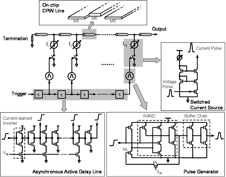
Fig.2 shows a 10-tap DWG prototype implemented in a 0.18um standard digital CMOS technology. It uses an active delay line for trigger distribution, digital pulse generator for basis pulse generation, switched current sources for pulse amplitude control, and an on-chip transmission line for pulse combining.
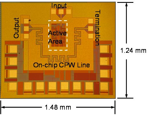
The prototype DAWG was fabricated in a commercial 0.18um standard digital CMOS technology with low-resistivity substrate. The chip micrograph is shown in Fig.3. The chip size is 1.48mmx1.24mm, including pads. The active area is 0.68mmx0.5mm.
Measurement Results
The prototype DWG is characterized in time domain using a 50~GHz sampling oscilloscope. A 500~MHz sinusoidal signal from a continuous-wave (CW) source is used as the input trigger. The delay uniformity of all ten taps can be observed in Fig.4. They are measured between the middle points of rise edges. The average tap delay is 104~ps with a standard deviation of 15.1ps, which corresponds to a sample rate of 10GS/s.
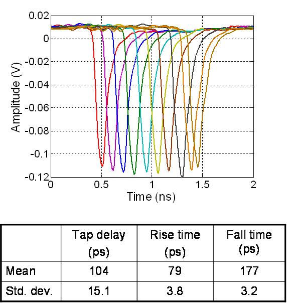
Fig.5 shows synthesized sinusoidal waveforms and UWB waveforms with their frequency spectra. The first sinusoidal waveform has a fundamental frequency of 930MHz, and the SFDR is 30dBc. The second sinusoidal has a peak frequency at 4.5GHz, close to the Nyquist rate. The UWB pulses include monocycle, doublet and 5th Gaussian derivative, with the center frequency from 2 to 4GHz. Note that we use a sinusoidal (CW) signal source as the trigger in these tests. Pulse repetition rate up to 1.1GHz can be sustained, which shows that a DWG can be used for high data-rate applications. Since the prototype is designed with single-polarity pulses, these pulses are generated with dc offset on-chip (ac coupled off-chip), which causes some asymmetry in the waveform.
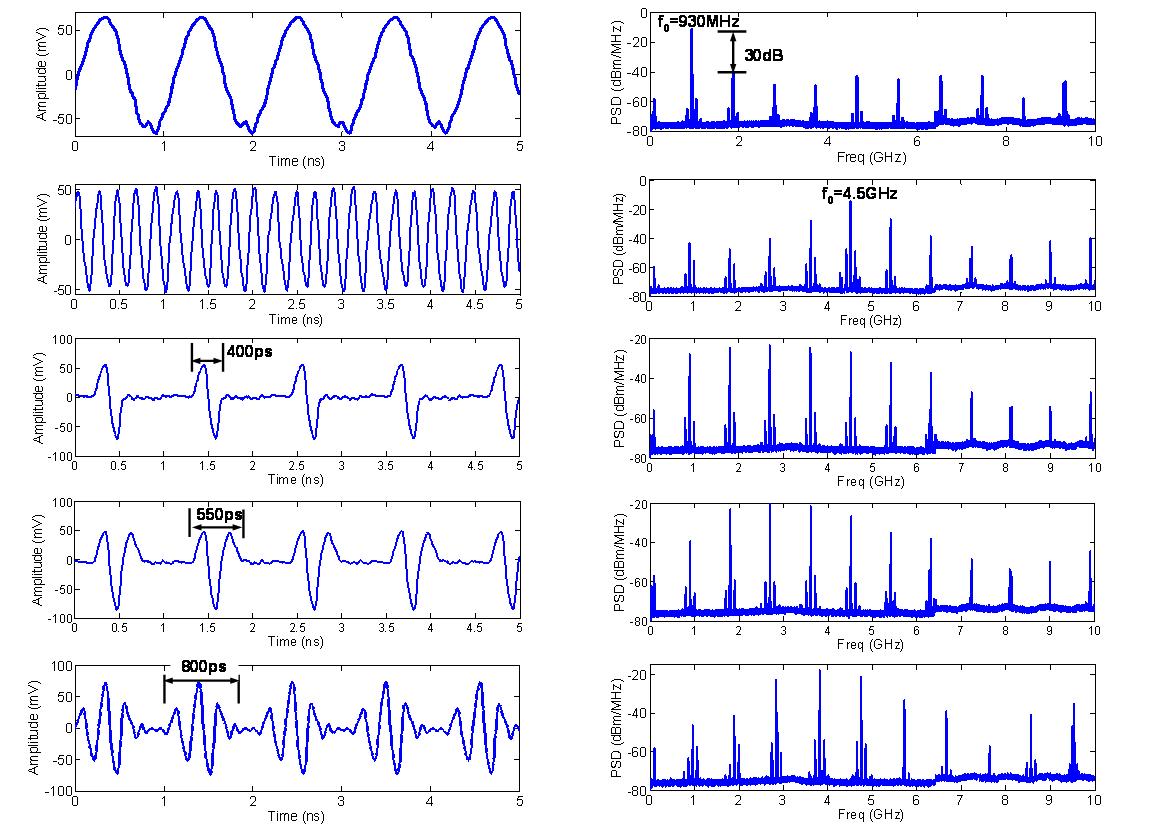
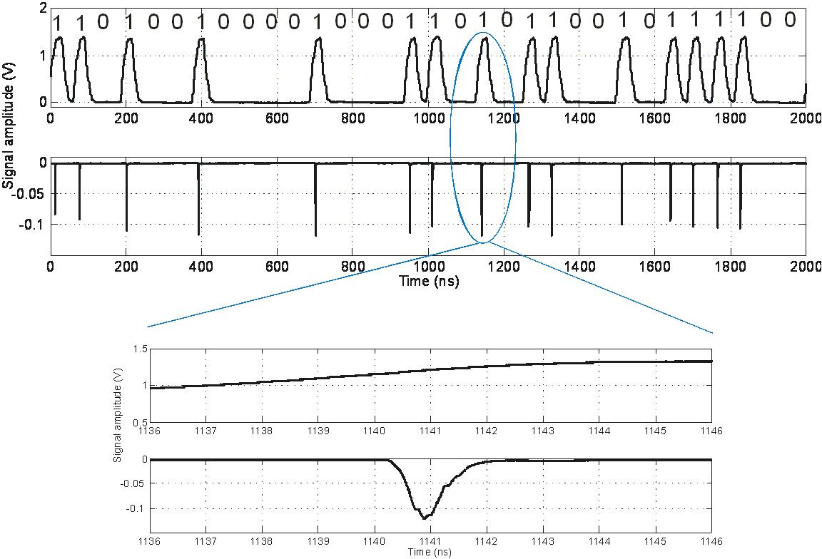
Fig.6 shows the on-off keying modulation of the prototype driven by a 32-bit, 16Mbps pseudo random bit stream (PRBS) with a Gaussian basis pulse. The small fluctuation on the waveform amplitude is caused by the limited number of sampling points (4096pts) in the measurement window. A DWG’s power consumption is proportional to the pulse repetition frequency (PRF), which is about 25mW at 500MHz and 50mW at 1GHz. The prototype performance is summarized and compared with other reported work in Fig.~\ref{fig:performance}.
References
[1] M.Z. Win and R.A Scholtz, “Ultra-wide bandwidth time-hopping spread-spectrum impulse radio for wireless multiple-access communications”, IEEE Transactions on Communications, 48.2423-2426, Apr. 2000.
[2] Y. Zhu, J.D. Zuegel, J.R. Marciante, H. Wu, “A 10GS/s Distributed Waveform Generator for Subnanosecond Pulse Generation and Modulation in 0.18um standard Digital CMOS”, in Proc. IEEE Radio Freq. Integrated Circuit Symp. , 2007.