Ultrafast pulse shaping for OMEGA laser system
CAEPS: Continuous Arbitrary Electrical Pulse Shaping
CAEPS is a joint project with Dr. Jonathan Zuegel’s Laser Technology Development Group at the Laboratory for Laser Energetics (LLE). In this project, we investigate new methods to adaptively generate and/or shape nanosecond electrical pulses with picosecond time resolution and good dynamic range. The developed prototype will be used for pulse shaping in OMEGA Laser System at LLE. The technologies will also be applied in wideband communications, radar, high-speed instrumentation, and other ultrafast pulse systems. This project is part of our research efforts on adaptive wideband circuits.
Pulse Shaping in OMEGA
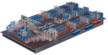
OMEGA (Fig.1) at LLE is one of the most powerful and highest energy lasers in the world. It is a 60-beam pulsed ultraviolet (UV) neodymium glass laser. Its 60 laser beams focus up to 40 kilojoule of optical energy onto a target that measures less than 1 millimeter in diameter in approximately 1 nanosecond, which corresponds to about 40 terawatts in terms of power. OMEGA provides a unique capability to conduct inertial-confinement, direct-drive, laser-induced fusion experiments and other basic physics experiments in support of the National Inertial Confinement Fusion (ICF) program. The ultimate goal of LLE experimental program on OMEGA is to achieve controlled nuclear fusion, which will provide a safe, clean, and virtually unlimited source of energy. OMEGA is also used to develop new materials and laser technologies, and other advanced technologies related to high-energy-density phenomena.
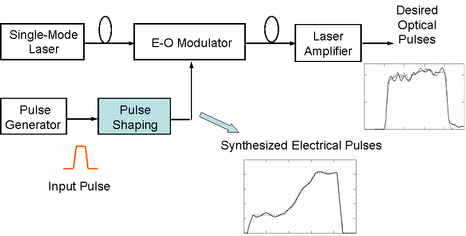
Based on fusion experiment requirements, OMEGA needs to generate optical pulses with various temporal pulse shapes. This is done by inserting an electric-optical modulator in the laser system, and applying a shaped electrical pulse to modulate the optical pulse, as shown in Fig.2. The electrical pulse is generated by a pulse generator with a fixed pulse shape, and then changed to the specified pulse shape by a pulse shaping circuit. The shaped electrical pulse needs 50-ps time resolution and 20-dB dynamic range. The pulse shape is usually different from shot to shot, and hence it is highly desirable that the pulse shaping circuit can be reconfigured adaptively.
Currently, pulse shaping in OMEGA is implemented as an aperture-coupled stripline (ACSL) module, shown in Fig.3. There are two transmission lines (specifically, striplines) in this module, one for the input pulse, and the other for the output. Both are terminated at one end. There is an opening (aperture) at the middle ground layer. When the input pulse propagates along the input line, it is coupled to the output line through the aperture. The aperture width determines the coupling strength, and its length corresponds to the output pulse duration. By designing the geometry of the coupling aperture, a specific electrical pulse shape can be generated [1].
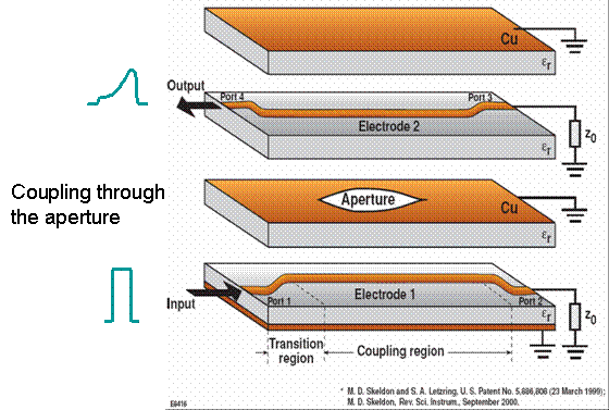
There are several limitations of an ACSL module. First, the module is implemented as an assembly of multiple printed circuit boards (PCB), and hence the mechanical tolerance in PCB fabrication and assembling limits the pulse shape precision, particularly its dynamic range. Second, a unique aperture design is required for each desired pulse shape and energy, which results in a significant overhead in design, fabrication, testing, and storage of ACSL modules. Most importantly, an ACSL module cannot be reconfigured once manufactured, and hence it is difficult to change the pulse shape in near real-time. In order to address these problems, active-controlled coupling is needed. This leads to the idea of using a distributed transversal filters (DTF) for reconfigurable electrical pulse shaping.
Distributed Transversal Filters
Distributed circuits such as traveling-wave amplifiers are widely used as microwave monolithic integrated circuits (MMIC) because of their unique wideband characteristics [2]. Fig.4 shows an integrated transversal filter using a distributed architecture [3-5]. It can be viewed as a traveling-wave amplifier with the output taking from the reverse direction. The input signal travels along the input transmission lines (gate-line), and is tapped by each gain stage in sequence (from left to right in Fig.4). The tapped signal is amplified by each gain cell by a gain proportional to the filter coefficient, and the output signals from all cells are power-combined on the output transmission lines (drain-line). The loaded transmission lines act as delay elements.

Such a distributed transversal filter (DTF) is essentially an finite-impulse-response (FIR) filter. Compared to conventional digital FIR filters, however, a DTF has some distinctive advantages: 1) it can achieve much larger bandwidth because its bandwidth is only limited by the cut-off frequency and loss of the loaded transmission lines. This corresponds to ultrafast rise and fall time for output pulses. 2) the filter coefficients can be easily and independently controlled by each gain cell, and thus it is inherently reconfigurable. 3) the delay between taps is not limited by the system clock cycle, and hence provide the design freedom in the pulse temporal resolution. 4) the power consumption can potentially be much lower since there is no power-hungry high-speed digital circuits.
CMOS DTF Prototype for Pulse Shaping
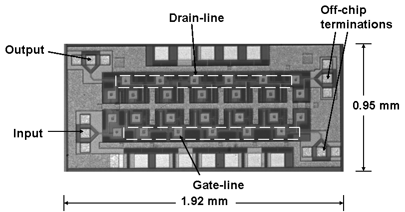
We have designed and fabricated a prototype DTF [6] using National Semiconductor’s 0.18um digital CMOS technology with a low-resistivity substrate. The detailed schematic is shown in Fig.5. It consists of two LC artificial transmission lines coupled through a number of gain cells. The total delay is specified by the target pulse width, and the delay per stage is set by the pulse temporal resolution. In this design, the delay is specified as 50 ps/tap, and 200 ps in total, which means the number of stages is 5. The chip occupies 1.92 mm by 0.95 mm (Fig.6). The power supply voltage is 2V.

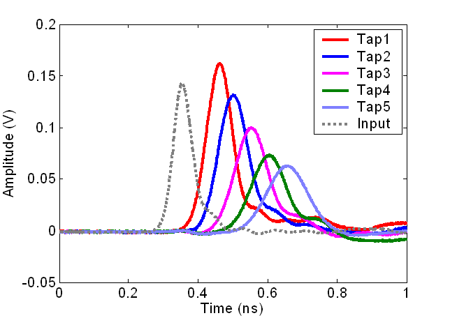
Impulse response of each tap (Fig.7) is measured using a Picosecond Pulse Labs 4500E pulse generator with 5210 impulse generator, which is very close to a Gaussian pulse with a pulse width (FWHM) of 40 ps. The interstage delays are measured at the middle point of the rising edge, which are 44.6 ps, 47.3 ps, 46.7 ps, 44.1 ps. This shows a good match with the design value of 50 ps. The delays also have good uniformity for all five taps, which is an obvious advantage of integrated circuit solutions compared to discrete implementations.
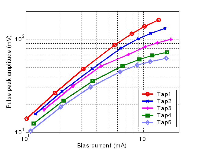
The gain control of each tap is shown in Fig.8, which is tuned by changing through a current mirror in each cell. The curves are plotted in log-log scales to better show the linearity across the dynamic range of 8-10 dB. The tuning curves show some nonlinearity for large bias current because of gain saturation. This relation between pulse amplitude and bias current is then used in the pulse synthesis to correct this nonlinear effect.
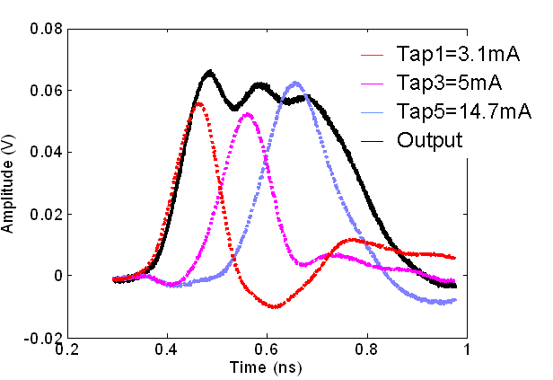
The filter can adequately synthesize a square waveform with 80 ps rise time and 380 ps pulse width (FWHM), as shown in Fig.9. The total power consumption in this case is 95 mW.
References
[1] Mark D. Skeldon, “Optical pulse-shaping system based on an electro-optic modulator driven by an aperture-coupled-stripline electrical-waveform generator”, J. Opt. Soc. Am. B, vol. 19, No. 10, pp.2423-2426, 2002.
[2] E.L. Ginzton, W.R. Hewlett, J.H. Jasberg and J.D. Noe, “Distributed amplification”, Proc. IRE, vol.36, pp. 956-969, Aug 1948.
[3] W. Jutzi, “Microwave bandwidth active transversal filter concept with MESFETs “, IEEE Trans. Microwave Theory Tech., vol.19, pp. 760-767, Sep. 1971.
[4] C. Rauscher, “Microwave active filters based on transversal and recursive principles”, IEEE Trans. Microwave Theory Tech., vol.33, pp. 1350-1360, Dec. 1985.
[5] H. Wu, J. Tierno, P. Pepeljugoski, J. Schaub, S. Gowda, J. Kash, and A. Hajimiri, “Integrated transversal equalizers in high-speed fiber-optic systems”, IEEE J. Solid-State Circuits, vol.38, pp. 2131-2137, Dec. 2003.
[6] Y. Zhu, J.D. Zuegel, J.R. Marciante, H. Wu, “A 0.18um CMOS Distributed Transversal Filter for Subnanosecond Pulse Synthesis”, in Proc. IEEE Radio and Wireless Symp., pp. 563-566, Jan. 2006.