High-speed silicon photodetectors in standard CMOS
High-Speed Silicon Photodetectors in Standard CMOS
This is a joint project with Dr. Jonathan Zuegel’s Laser Technology Development Group and Dr. Roman Sobolewski’s Ultrafast Quantum Laboratory. at the Laboratory for Laser Energetics (LLE) In this project, we study integrated silicon photodiodes (PDs), presenting a new PIN PD structure with deep n-well (DNW). Prototype PDs were fabricated in a standard CMOS technology, and their dc, impulse and frequency responses were characterized. A 70×70-µm² PD with the new structure achieved 3-dB bandwidth of 2.2 GHz in small-signal at 5-V bias voltage. The bandwidth increased up to 3.1 GHz at 15 V. The responsivity of the PD was 0.14 A/W at low bias voltages and it increased upto 0.4 A/W at 16 V. These PDs can be used in integrated optical receivers for short-haul communications. Especially, as the number of PDs increases with the deployment of parallel optics and or wavelength division multiplexing to improve aggregated system bandwidth, fully-integrated high-speed PDs will reduce the interconnection bottleneck between PDs and receiver electronics.
The performance of a integrated silicon PD depends on both the material properties, such as absorption coefficient and mobility of carriers, and optical wavelength. Besides these, it is strongly dependent on the device structure, which is limited dielectric values, layer thicknesses, and doping profiles. For example, a conventional vertical PD designed in bulk CMOS process achieves larger responsivity but smaller bandwidth, compared to a same size PD implemented in epitaxial CMOS process, where the substrate consists of a low doped epitaxial layer on top of a heavily doped substrate. Consedering the transport mechanisms of electrons and holes, we know that a highly doped p-type material will help the recombination of electrons [1]. This mechanism in a epi-CMOS PD helps the recombination of the carriers generated deep inside the substrate, which has very weak or no electric field at all, and hense causes these carriers to either drift or diffuse slowly. The recombination of these slow transport components increase the bandwidth of the device, whereas reduce the responsivity. Our prototype PDs are implemented in epi-CMOS technology.
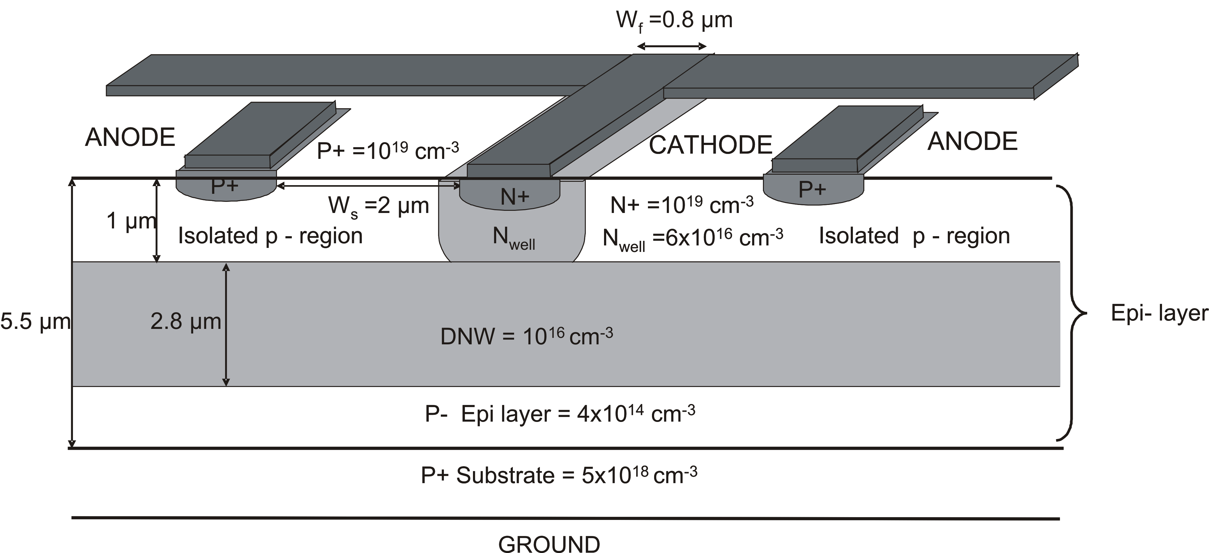
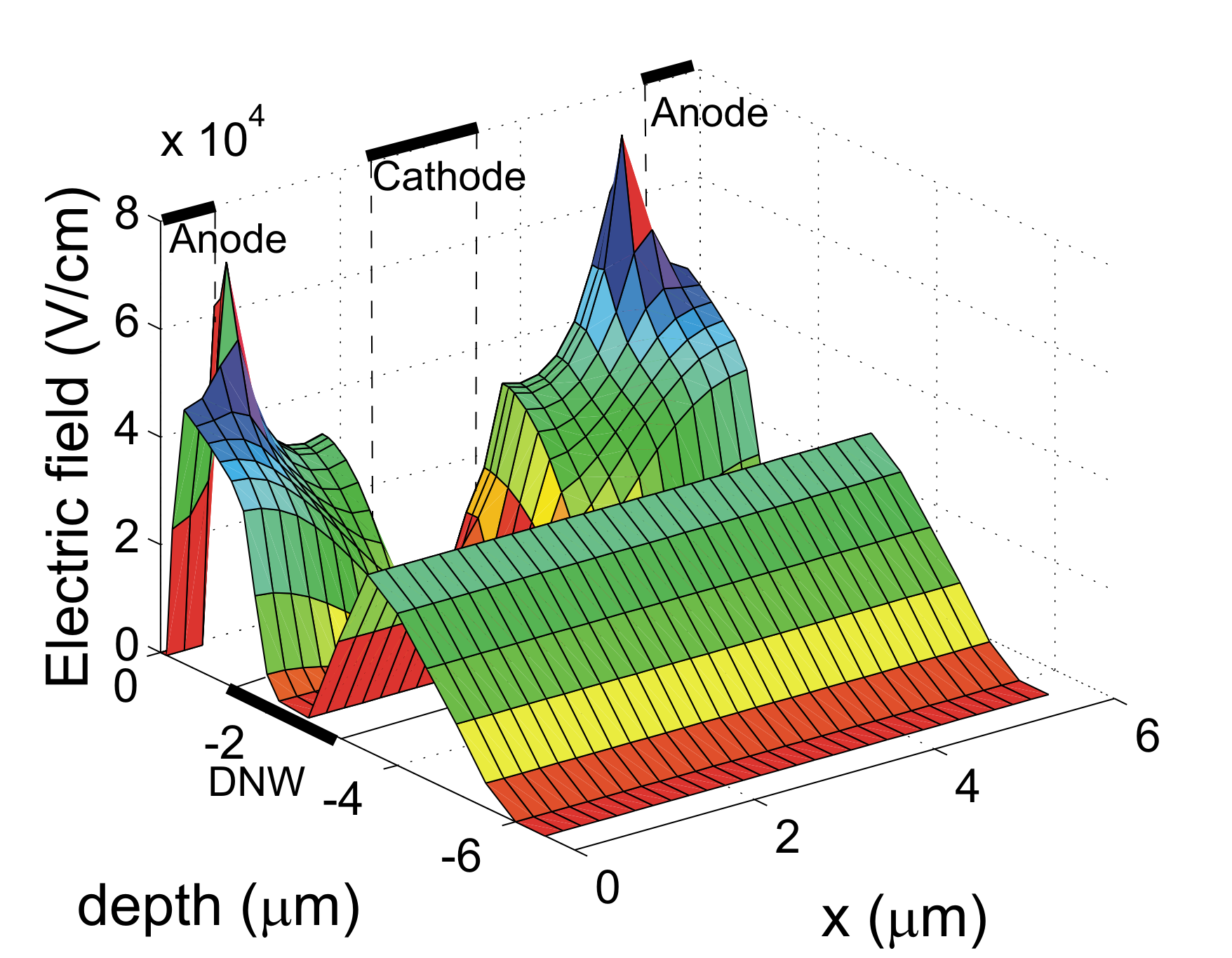
DNW is an n-type layer buried inside the expitaxial layer in epi-CMOS technologies. This layer is typically used for improving transistor isolation from the substrate and reduce the substrate noise coupling in mixed-signal and RF circuits. The new PD structure (Fig.1) can be implemeted by adding DNW to a lateral PIN PD structure, connecting all the n regions together. This structure creates two seperate junctions: one with the isolated p-region on the top and the other with the epi layer and the substrate on the bottom. The upper one becomes a hybrid lateral-vertical PIN structure with a thinner depletion region than without the DNW. Whereas, the bottom PN junction increases the electric field magnitude, and hence the drift speed of the generated carriers close to the epi/substrate interface. The electric field distribution inside a finger segment is shown in Fig.2. The heavily doped substrate recombines the carriers generated deep in the substrate reducing the diffusion current contribution, therefore enhancing the bandwidth of the device.
Measurement Results
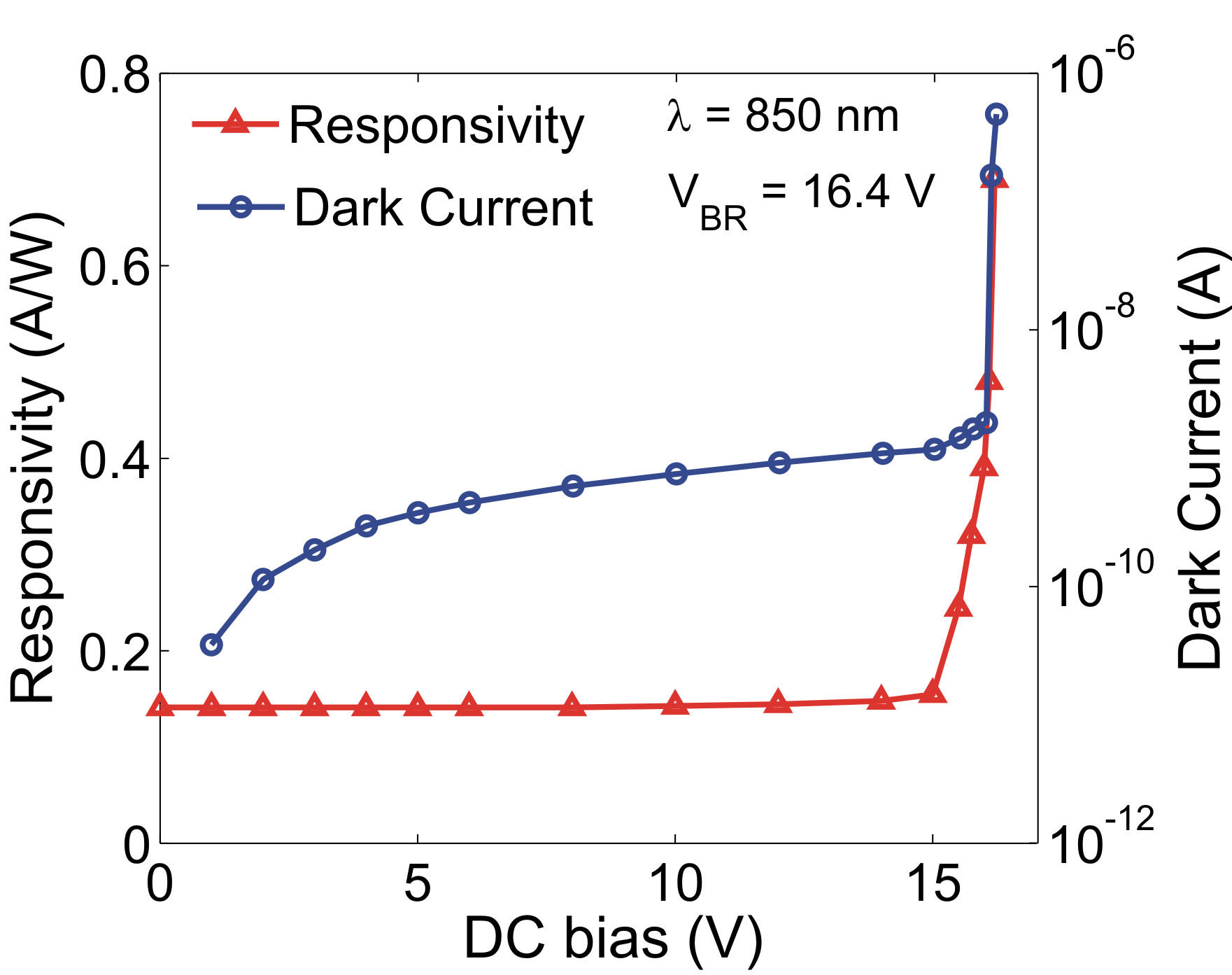
In the dc measurement, a high speed VCSEL (Finisar HFE8004-103), with an optical power of 2 mW, was used as the light source at 850 nm. The emitted light was collimated and then focused onto the PD with two stages of lens. The spot size was adjusted to precisely cover the active region. A commercial silicon PIN diode (EOT ET-2030), with a bandwidth of 1.2 GHz and responsivity of 0.4 A/W at 850 nm, was used as a calibration reference for the optical power of the VCSEL. At 5-V the responsivity of the PD was 0.14 A/W with a quantum efficiency of 20% (Fig.3). At 16.2 V, it increased up to 0.4 A/W, due to impact ionization. The dark current was below 1 nA until 13 V and 1 µA until 16.2 V.
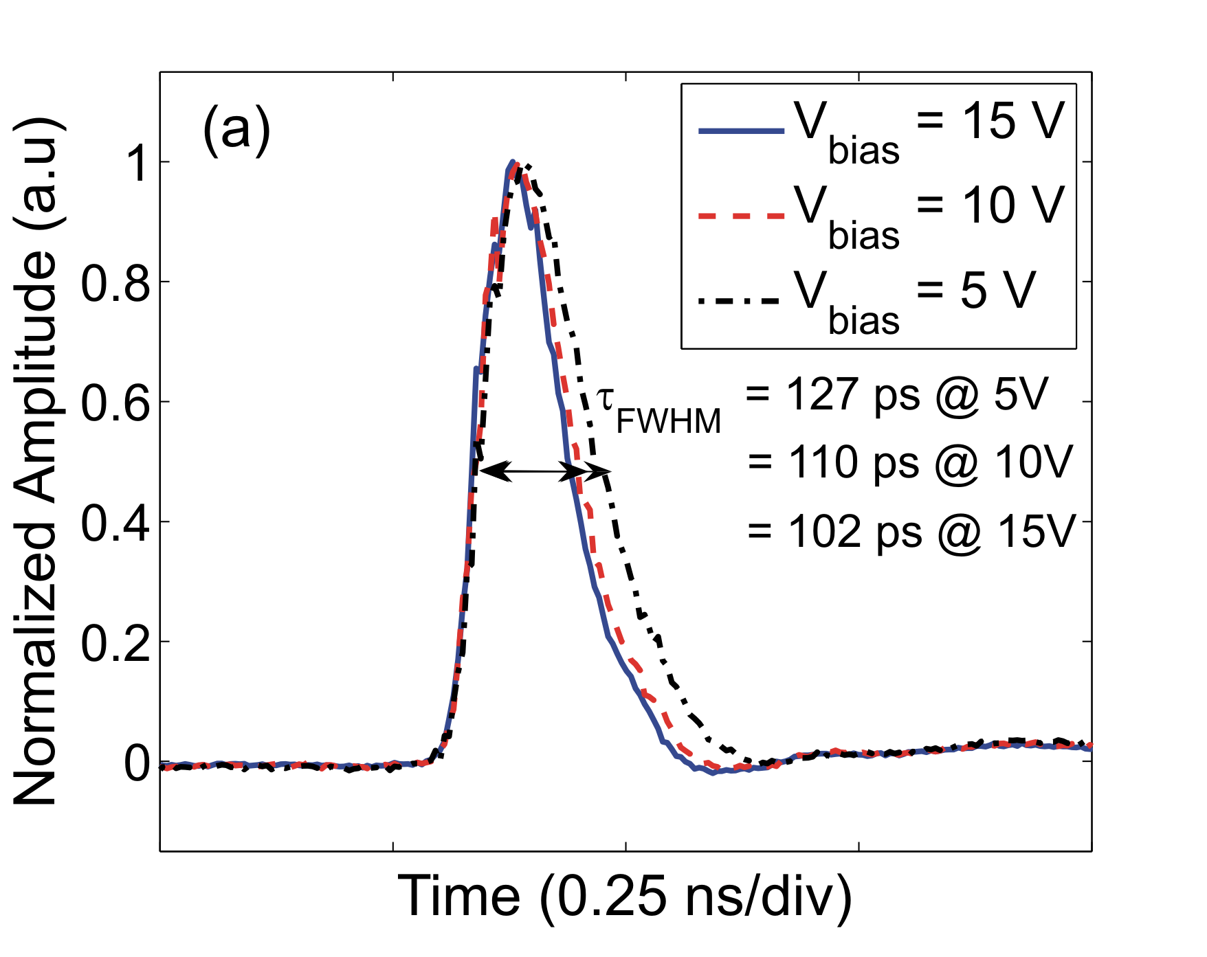
In the impulse response measurements, a tunable modelocked Ti&sub2:Al&sub3 femtosecond pulsed laser, operating between 700 and 1000 nm, was used as the light source with a repetition rate of 76 MHz. The pulse width was 100-fs, and could be treated as an impulse function in the PD measurements. The output of the PDs was fed into a digital sampling oscilloscope with a 3-dB bandwidth of 20 GHz. The average incident power on the PD was 0.27 mW at 850 nm, which corresponds to a peak power of 33.75 W and optical pulse energy of 3.55 pJ. The impulse response results were then converted to frequency response using discrete Fourier transform (DFT). The impulse response results showed that the full-width half maximum time constant of the PD was 127 ps at 5 V and it reduced down to 102 ps at 15 V (Fig.4). The fall time was 147 ps at 5 V and it reduced down to 114 ps at 15 V. The DFT spectra of the PD had 3-dB bandwidth of 2.08, 2.45 and 2.60 GHz, respectively.
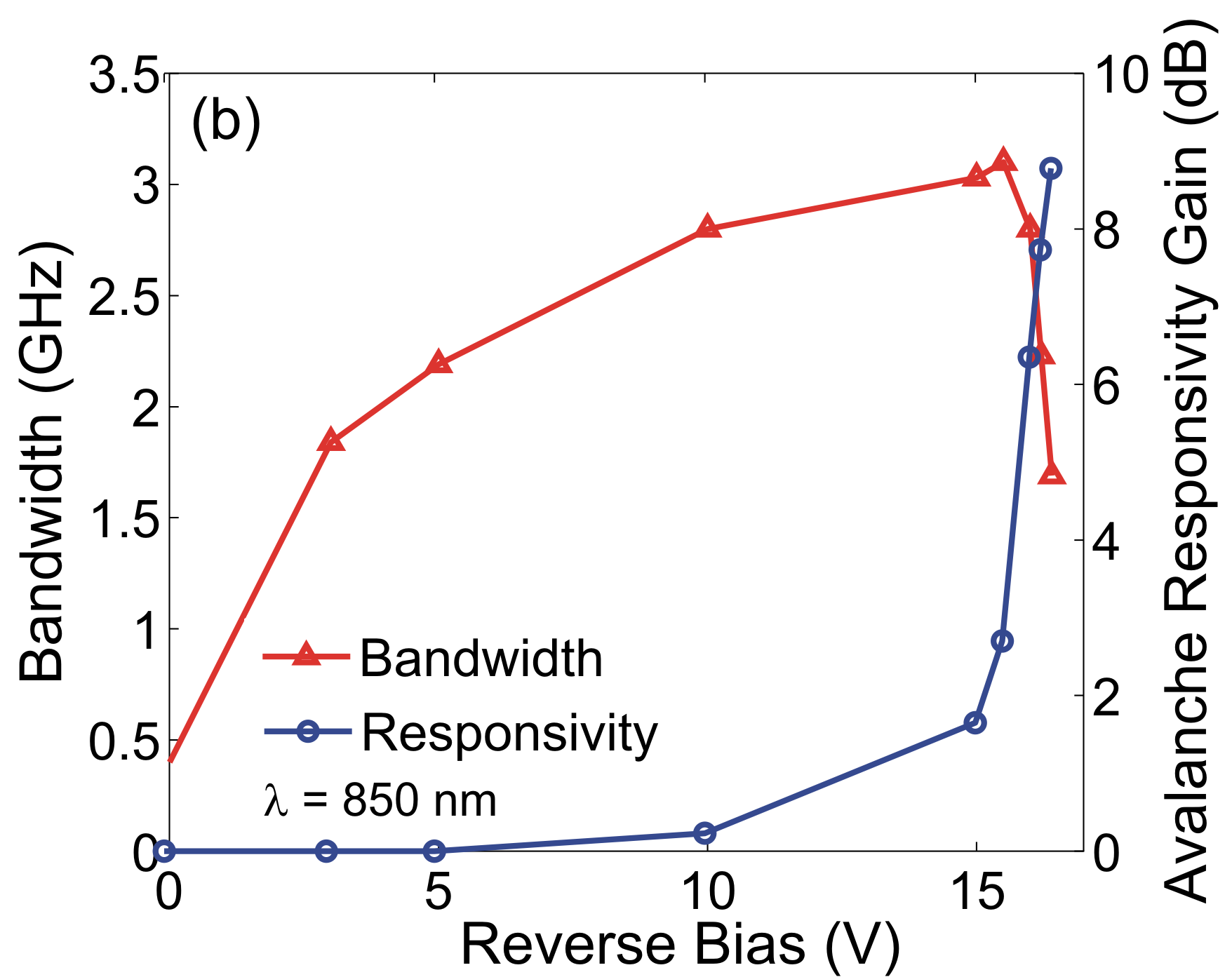
In the small-signal measurement, the same VCSEL as in the responsivity measurement was used. The bandwidth and the avalanche responsivity gain with respect to bias voltage is shown in Fig.5. As the bias voltage increases, the drift speed of the carriers increases due to the higher electric field in the active region. At high voltages such as 16 V, avalanche gain increases due to impact ionization of the carriers. At 16.2 V, the PD could achieve 0.4 A/W with 2.8 Ghz small signal bandwidth, with a dark current value of 0.6 µA. The PD could achieve its largest bandwdith at 15.5 V with a responsivity gain of 3 dB with a dark current value of 2 nA.
References
[1] I.-Y. Leu, A. Neugrosschel, “Minority-Carrier Transport Parameters in Heavily Doped p-type Silicon at 296 and 77 K”, IEEE Trans. Electron Devices, vol. 40, No. 10, pp.1872-1875, 1993.
[2] B. Ciftcioglu, J. Zhang, L. Zhang, J.R. Marciante, J.D. Zuegel, R. Sobolewski, and H. Wu, “3-GHz Silicon Photodiodes Integrated in a 0.18-um CMOS Technology”, IEEE Photonic Technology Letters, vol. 20, no. 24, pp. 2069-2071, Dec. 2008..