Injection-locked clocking
Injection-Locked Clocking
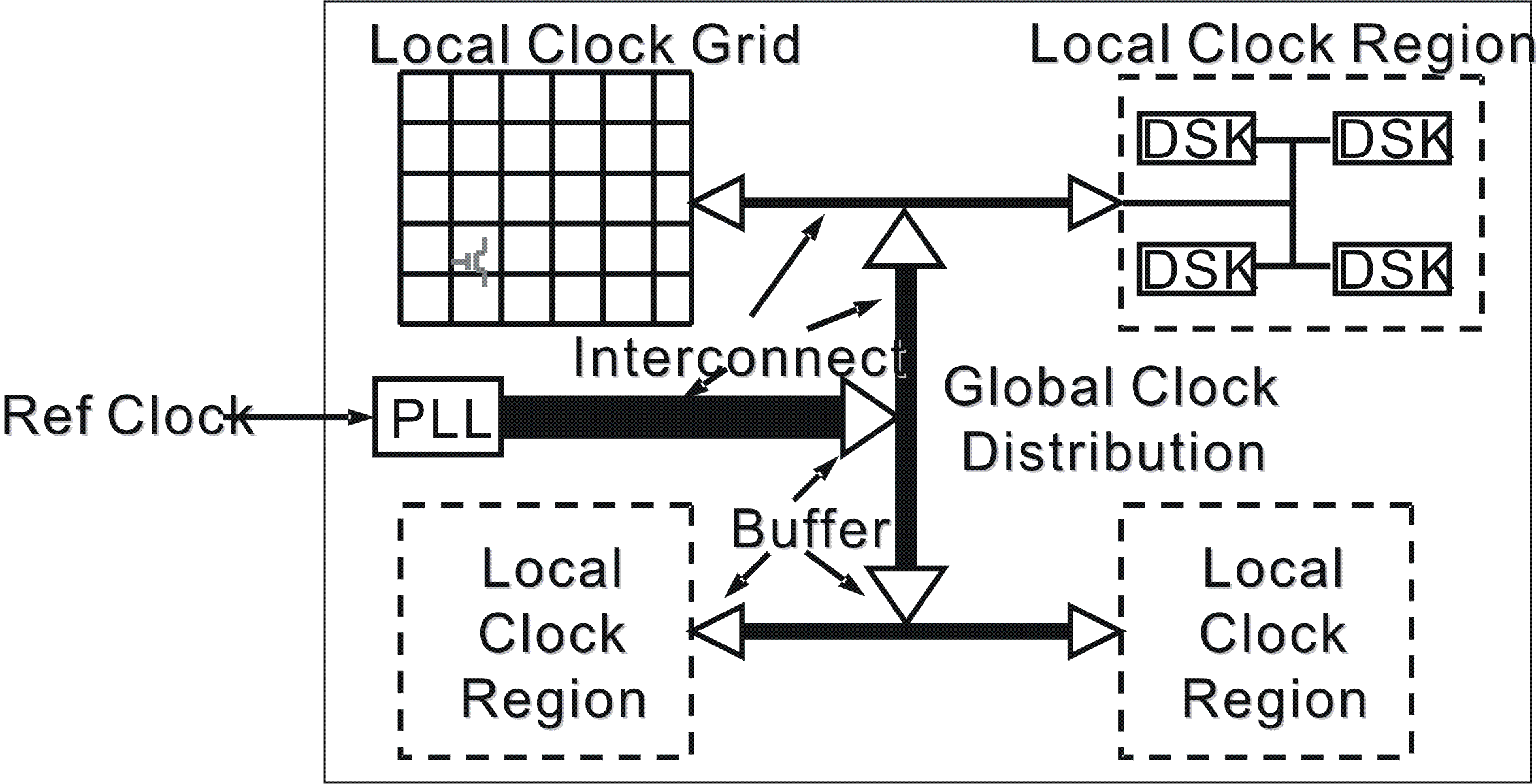
Clock distribution will increasingly be one of the most challenging tasks in microprocessors and other high-speed VLSIs. The conventional clock distribution is based on buffered chain structure, with techniques like H-tree and grid to reduce the skew (Fig.1). However, if current clocking schemes continue to be used, it is expected that skew and jitter will consume an increasingly large portion of each clock cycle, and hence the time available for critical path will eventually be less than the technology-allowed minimum delay beyond the 32nm node in 2013. This will largely defeat the purpose of any further clock speed increase. In the meantime, the power consumption in clock distribution networks has also become a serious problem. Currently, about 40% of total power consumption of a high-performance microprocessor is used by the clocking circuitry [1]. As both clock speed and transistor count increase, the projected power consumption of a high-performance microprocessor will exceed the power density limit set by packaging. Therefore, we need a new clocking solution that can achieve better skew and jitter performance while consuming less power.
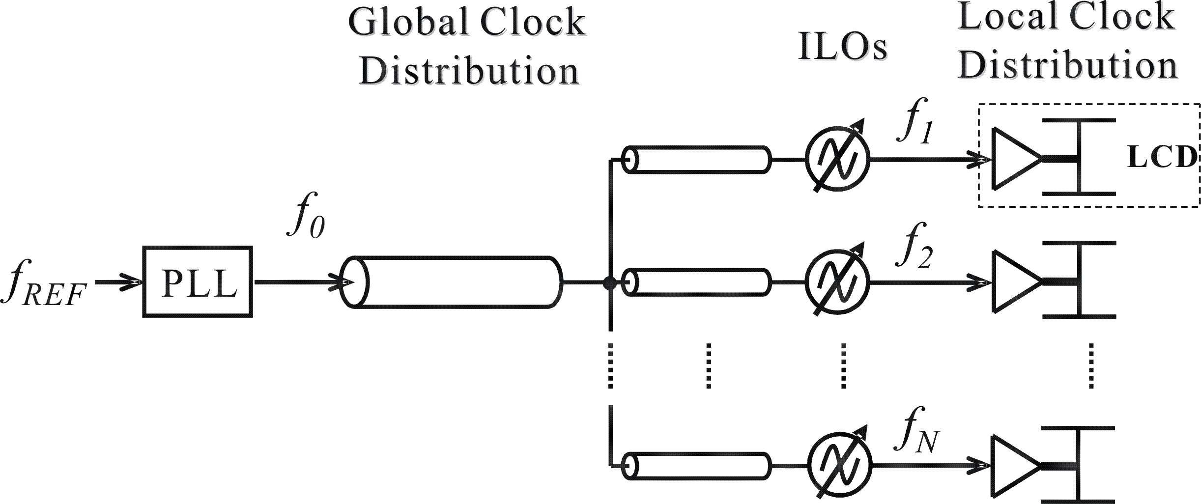
We propose a new clock distribution scheme which utilizes injection-locked oscillators as the local clock generators. The new scheme has better jitter performance, consumes less power, and provides built-in deskew capability. Fig.2 shows the proposed new clocking scheme. We use injection-locked oscillators (ILOs) to generate local clocks, which are synchronized to the global clock through injection locking [2]. Note that this is different from resonant clocking [3], where all the oscillators are coupled together. Further, ILOs can be constructed as frequency multipliers[4] or dividers [5][6], and hence this scheme enables local clock domains at higher (n f0) or lower speed (f0/m) than the global clock (f0). Such a global-local clocking scheme with multiple-speed local clocks offers significant improvements over conventional single-speed clocking scheme in terms of power consumption, skew, and jitter.
Power Efficiency
The combination of a low-speed global clock and high-speed local clocks can reduce the power consumption in the global clock distribution network. The conventional approach, however, would require multiple power-hungry phase-locked loops (PLL) for frequency multiplication. An ILO consumes much less power than a PLL because of their circuit simplicity [6].
Running at the same clock speed, injection-locked clocking can also significantly reduce the power consumption in the global clock distribution network compared to conventional clocking. As a synchronized oscillator, an ILO effectively has very large voltage gain when the injection signal amplitude is small, while the gain of an inverter is much smaller. In other words, ILOs have higher sensitivity than buffering inverters. Therefore, the clock signal amplitude can be much smaller in the new clocking scheme, which means less power loss on the global-clock distribution interconnects. The number of clock buffers can also be reduced, which lowers the power consumption further.
Built-in Deskew Capability
Because the number of buffers is reduced in the new clocking scheme, one of the major sources of skew, clock buffer mismatch, is also reduced compared to conventional clocking. In addition, the new scheme provides a possible method for deskewing local clocks. Similar to the phase error in a PLL, the phase difference between the input and output signals of an ILO is a function of their frequency difference. When the center frequency of an ILO is tuned, therefore, the phase of the output signal will shift accordingly. The phase shift is a monotonic function of the frequency shift, and the function is quite linear within the locking range [7][8]. This phase tunability enables ILOs to also serve as built-in “deskew buffers”. In turn, removing dedicated deskew buffers not only saves power, but also reduces their vulnerability to power supply noise.
Jitter Suppression
Reduced number of clock buffers also means less pick-up of power supply and substrate noise and hence less jitter generation and accumulation. In addition, similar to a PLL, the ILO shows a high-pass filtering for the phase noise due to the internal noise sources. Because of the large “loop bandwidth” of an ILO, the internal phase noise of the oscillator is largely suppressed, and has little effect on the ILO jitter [6]. For jitter transfer, phase noise from the input signal at large offset frequency is attenuated because of the low-pass noise transfer function similar to a PLL. Because short-term (cycle-to-cycle) jitter matters in clocking, which is largely determined by the phase noise at large offset frequency [9], an ILO can potentially suppress the input signal jitter. Overall, injection-locked clocking is likely to achieve better jitter performance than conventional clocking.
Test Chip
A 4GHz test chip is designed and implemented in a standard 0.18um digital CMOS technology with low-resistivity substrate.Input transformer and symmetric inductor of the ILO are implemented on Metal 5(Fig.3a). Transformer has a k factor of 0.6 and inductor has a quality factor of 4, both at 4GHz. The switched capacitor array was designed with capacitance ratio of 1:2:4:8:16 to enable a 5-bit binary tuning. Large capacitors are realized by combining multiple of the minimum-sized unit capacitors to ensure linearity.
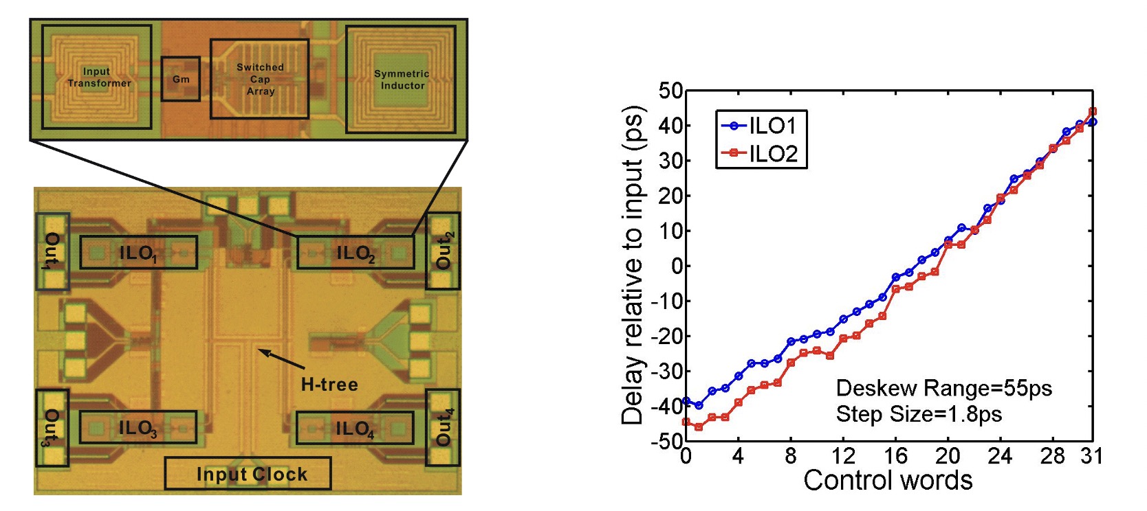
Four ILOs are placed as 4 local clock regenerators at the leaves of a 3-section H-tree, which mimics the global clock distribution network in real microprocessors. H-tree dimensions are 400um, 100um and 250um for 3 sections, respectively. The root of the H-tree is directly connected to a ground-signal-ground (GSG) pad to facilitate testing. The H-tree is constructed using coplanar waveguide (CPW) transmission lines. Bottom shield is used to reduce substrate coupling in a real microprocessor environment. A differential open-drain buffer is used at each ILO output to drive the 50-ohm test port. The whole test chip occupies an area of 1.5 by 1.8 mm2. Each ILO uses only 0.37 by 0.1 mm2.
In the measurement, the input is a sinusoidal signal from a continuous-wave (CW) signal generator. Output clock spectrums are measured for each ILO. The clean spectrum and low harmonic contents proves that injection locking is quite efficient. Locking ranges are measured with different input signal amplitude. Up to 12% locking range are achieved for all the ILOs when input amplitude is about 0.8V at the root of the H-tree.
Output waveforms for different tuning conditions were recorded and their zero crossing indicated their phase shift information. Phase shift tuning of two ILOs in the ILC are measured at the same time for comparison purpose. After calibrating out their cable mismatch and referring the phase to that of the center tuning point of one of the ILOs, the phase tuning curves are plotted in Fig.3b. The result shows that a phase tuning range up to 80o is achieved, which corresponds to 55ps delay tuning range with a step size of 1.8ps in time domain.
Phase noise of both signal generator and ILC output are also measured. From the comparison, the ILO output phase noise tracks exact the input phase noise up to 600 KHz. A self-triggered jitter measurement [9] was made for both the signal source and ILC output to characterize their jitter profiles. After removing the jitter introduced by the triggering circuit, the effective rms jitters versus measurement time for both signal source and ILC output are plotted. From the comparison, only 0.03ps of cycle-to-cycle jitter is added by the ILC network, which corresponding to 0.012% of the clock cycle, thanks to the noise filtering effect of the ILO. The power consumption for each ILO is only 0.95mW under 1V power supply voltage. Each open drain buffer burns 4.2mW from 1.5V Vdd.
For more details on this project, please see our TVLSI paper and the accompanying technical report here.
References
[1]V. Tiwari et al., “Reducing Power in High-performance Microprocessors,” Design Automation Conference (DAC), pages 732-737, 1998.
[2]R. Adler, “A Study of Locking Phenomena in Oscillators” Proc. IRE, vol.34, pp. 351-357, June 1946
[3]S.C. Chan, K.L. Shepard, and P.J. Restle, “1.1 to 1.6GHz DistributedDifferential Oscillator Global Clock Network,” IEEE Int. Solid-State Circuits Conf. Dig. Tech. Papers, pages 518-519, 2005.
[4]K. Kamogawa, T. Tokumitsu, and M. Aikawa, “Injection-Locked Oscillator Chain: A Possible Solution to Millimeter-Wave MMIC Synthesizers,” IEEE Trans. Microwave Theory Tech., 45(9):1578-1584, Sept. 1997.
[5]H. Rategh and T. H. Lee, “Superharmonic Injection-Locked Frequency Dividers,” IEEE J. Solid-State Circuits, vol. 34, pp 813-821, June, 1999.
[6]H. Wu and A. Hajimiri, “A 19GHz, 0.5mW, 0.35um CMOS Frequency Divider with Shunt-Peaking Locking-Range Enhancement,” IEEE ISSCC Dig. Tech. Papers, pp.412-413, Feb., 2001.
[7]L. Zhang, B. Ciftcioglu, M. Huang, and H. Wu, “Injection-Locked Clocking: A New GHz Clock Distribution Scheme,” IEEE Custom Integrated Circuits Conf. Dig. Tech. Papers, pages 785-788, 2006.
[8]L. Zhang, B. Ciftcioglu, and H. Wu, “A 1V, 1mW, 4GHz Injection-Locked Oscillator for High-Performance Clocking,” IEEE Custom Integrated Circuits Conf. Dig. Tech. Papers, pages 309-312, 2007.
[9]A. Hajimiri, S. Limotyrakis, and T.H. Lee, “Jitter and Phase Noise of Ring Oscillators,” IEEE J. Solid-State Circuits, 34(6):896-909, June 1999.