Nicholas Achuthan
Mentors
Professors Pablo Postigo and Jaime Cardenas
Abstract
Single photon emitters (SPEs) are a key building block for integrated quantum photonic circuits, but current implementations rely on heterogeneous integration of quantum emitters and waveguide architecture, leading to high coupling losses. Intrinsic, defect-based single photon emission has been recently demonstrated in silicon nitride, a low-loss material with exceptional waveguide properties. Such a development could enable the combination of quantum emitters and photonic circuitry into one platform, paving the way for low-loss quantum science on-chip. Here we discuss the experimental process of fabricating, processing, and testing silicon nitride samples for the presence of SPEs, including the effects of thermal annealing processes. Additionally, we investigate methods for Purcell enhancement of silicon nitride SPEs.
Introduction
Single photon emitters in silicon nitride are a new discovery pioneered by Vladimir Shalaev’s group at Purdue University. Though the exact nature of the emitters found is still unknown, the authors attributed the presence
of SPEs to a specific fabrication process: nitrogen-rich SiN is deposited onto an SiO2 substrate via high-density plasma chemical vapor deposition (HDPCVD), after which the samples are treated with rapid thermal annealing (RTA) at 1100◦ C for 2 minutes in nitrogen atmosphere1. In this
work, we use the findings from the above literature as a starting point to observe the emitters firsthand.
Methods
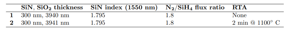
The SiN samples we investigated were fabricated at Cornell Nanoscale Facility (CNF) by Cardenas Lab PhD student Yi Zhang. For this work, we deposit 300 nm of non-stoichiometric silicon
nitride using HDPCVD over 4 µm of thermally grown silicon dioxide on a 4-inch diameter silicon wafer. Following the methods of Shalaev et al. [1], we adjust the gas flow ratio of nitrogen to silane to be 1.8 (18 sccm N2, 10 sccm SiH4) for a nitrogen-rich SiN film. Such a process has been shown
to reduce the background autofluorescence of the thin film [1]. Following the deposition process, we anneal one of the samples in an RTA system for 120 s at 1100◦C. The table below summarizes the properties of the two samples.
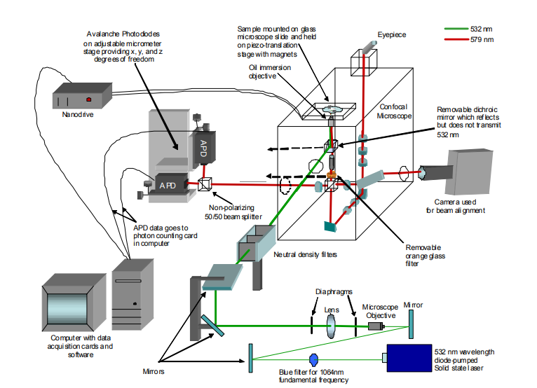
To test the samples for single photon emitters, we use confocal fluorescence microscopy.
Preliminary Results
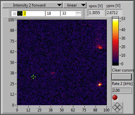
After our first round of testing, we observed only one significant localized emission feature from the RTA sample, and no features on the non-annealed sample. Our results at this point greatly differed from the reported emitter concentration (1-2 emitters per 10 × 10 µm^2 area) by Shalaev et al. [1].
.
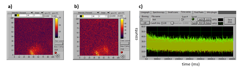
scan of the RTA sample. a) Scan from APD 1 and b) scan from APD 2. c) Counts vs. time for the observed emitter, showing noisy but stable emission. Excitation power set to 5.6 mW.
The vast majority of scans on both the annealed and non-annealed samples yielded no localized emission features. After accumulating an antibunching histogram for the above feature, we observed no prominent dip, meaning the feature is not a single photon source. We believe this feature could be some kind of dust or particulate on the sample, which can act as a localized emission point.
Further Testing and Results
Having found no convincing emitters in either the annealed or non-annealed wafer, we decided to study the effects of annealing in depth. In order to run experiments with as many conditions as possible, we cut our wafers into pieces using a diamond tip cleaving technique. The annealing
processes we considered were inspired by those performed in SiN SPE literature, as well as our own hypotheses on the emitter creation process. For example, if the origin of the emitters is from nanocrystal formation in the SiN matrix, annealing processes, their temperatures, and the time between consecutive treatments could play a role in emitter creation.
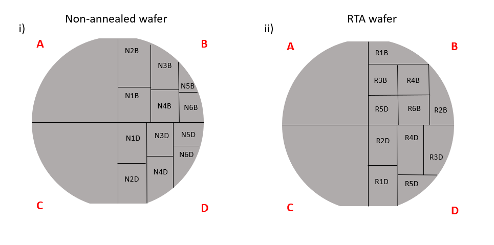
the wafer initially treated with an RTA process. Half of each wafer is preserved
intact for later testing.
A summary of the annealing processes performed is shown below:
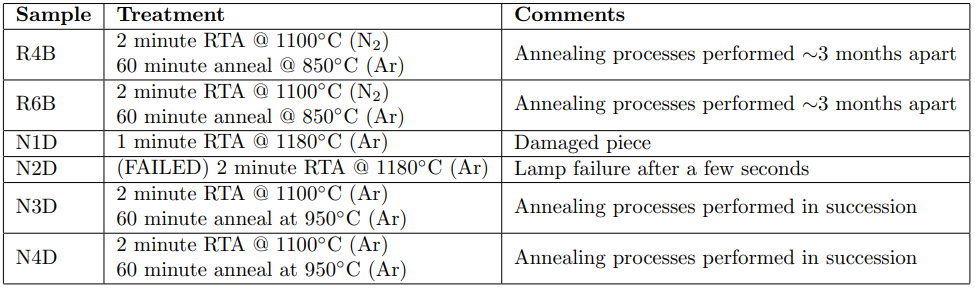
One of our samples (N1D) was damaged during the annealing process, shown in the figure below:
curve represents power delivered to heating lamps as a percentage of the maximum power. Red curve represents recorded temperature of furnace. b) Microscope image of thermally induced damage as a result of the RTA process shown
in a). c) Rectangular inscribing along the edges of a wafer piece to prevent
cracks from forming during RTA treatment. This was applied to pieces N3D
and N4D prior to RTA treatment, after which no cracks were visible.
After testing different annealing conditions, we were still unable to observe any localized emission features in any of the samples, suggesting the origin could be from a different process.
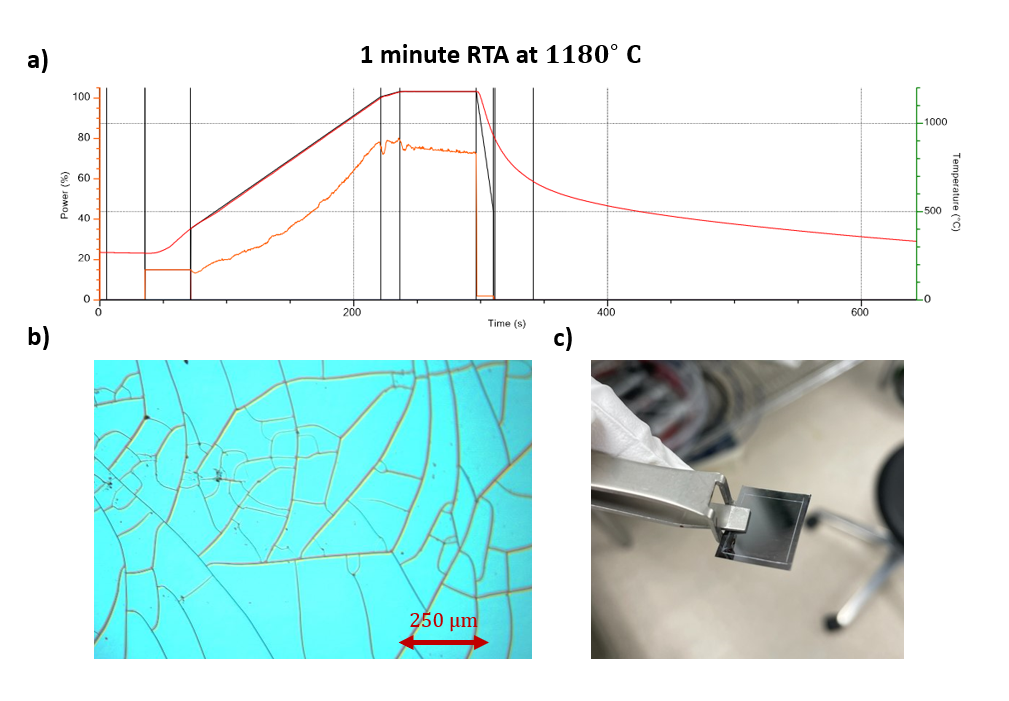
As an additional test, we look into the effect of inscribing focused ion beam marks on the samples. Focused ion beam (FIB) milling is a technique used for localized ablation of photonic integrated circuits, typically to make marks to locate specific areas of a wafer or chip. In SiN SPE literature, FIB marks are used as reference points to locate positions of different emitters.
In this study, we use gallium ion FIB to investigate the possibility that the marking process itself introduces SPEs into the film.
FIB marks [1]. b) A fluorescing FIB mark and neighboring SPEs [9]. c) Several
fluorescing FIB marks and circled SPE [10]. d) An image of one of our own
samples treated with FIB milling to create four X-shaped marks.
Further scans around the region of FIB marking led us to conclude that it was not responsible for single photon emitting defects. Interestingly, we noticed that regions treated with FIB exhibited a fluorescent intensity lower than that of the background, opposite the behavior depicted in the above figure. The area where the two FIB lines cross to form an X is also notably brighter, likely a result of a surface profile irregularity due to the double-pass of the ion beam.
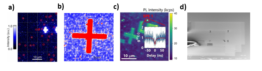
Despite observing no features in the SiN samples above, we did observe a fluorescent feature from a SiN sample deposited via low-pressure chemical vapor deposition (LPCVD). This sample did not originate from any of the wafers designed to produce SPEs, nor was it subject to any annealing
processes.
NA objective. Max count rate corresponds to an emitter brightness of ∼ 10
kcounts/s.
A complete characterization of this emitter has not yet been performed, so its origins are unknown. Further study, including spectral characterization and antibunching measurements, are required to accurately compare this emitter with SPEs reported in literature.
Photonic resonator CAD
As a theoretical portion of this project, we investigated the Purcell enhancement of single photon emitters in silicon nitride using nanophotonic cavities. The Purcell factor, which describes how an emitters brightness is amplified when placed in a resonating cavity, is critically dependent on the ratio of quality factor to mode volume of the resonators. For this section, we focus on the simulation of a 2 dimensional photonic crystal cavity (PCC) formed by a hexagonal array of air holes in silicon nitride. To calculate the quality factors and mode volumes of cavity resonances, we use the Q-finder utility from RSOFT.
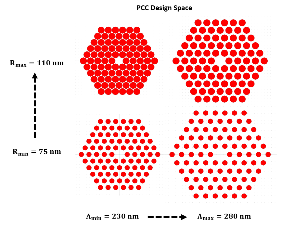
The radius of defects (air holes, red) ranges from 75 nm to 110 nm, while the
period of the defects arranged in a hexagonal lattice ranges from 230 nm to 280
nm.
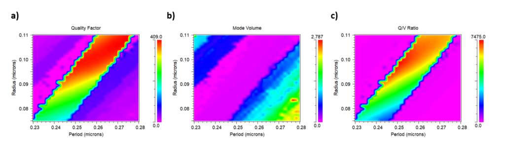
RSOFT. a) Quality factor of resonance. b) Mode volume of mode profile (dimensionless). c) Quality factor to mode volume ratio.
Our simulations show that there is a specific band in parameter space in which the cavity can support a low-loss resonant mode. Additionally, the quality factor maxima tend to overlap with areas of low mode volume, which is advantageous for maximizing the Q/V ratio. Ring resonators,
for example, tend to behave differently. Confining the mode to a smaller volume means making the bending radius of the ring tighter, inducing loss and lowering Q.
The Purcell enhancement of SiN emitters remains a challenge due to the non-deterministic nature of the emitter position. While SiN emitters have been successfully placed in waveguides [2], their integration has relied on having high enough emitter densities such that emitters end up in
the waveguide by chance. Alignment of an emitter into a small resonant mode of a cavity would require a higher degree of precision.
Conclusion
The recent discovery of room temperature single photon emitters in silicon nitride is a promising avenue towards low-loss photonic integrated circuits for quantum applications. We deposited SiN on SiO2 films following procedures developed in SiN SPE literature [1], characterized the autofluorescence spectrum, and studied the impact of different annealing processes. We additionally tested the effect of FIB milling on sample fluorescence, concluding that it was not responsible for SPE
creation. Finally, we studied the dynamics between quality factor and mode volume of a 2D SiN photonic crystal cavity for Purcell enhancement of SiN SPEs. Our studies have underscored the difficulty of replicating work from other groups. In our samples fabricated to match the methods of Shalaev et al., we observed no SPEs, contrary to previously
reported emitter densities of 1-2 per 10 × 10 μm^2 [1]. A myriad of variables in the nanofabrication process can lead to different thin film properties, a complete list of which is never included in published papers. Consequently, identical replication is nearly impossible. We suspect that the origin of the reported emitters could be unique to specific fabrication conditions, such as the presence of a contaminant in one of the fabrication steps. Surprisingly, the most promising emission feature we observed was on an unannealed LPCVD film of near-stoichiometric silicon nitride. Further testing is required to characterize this source as an SPE; if it is, we may discover that SPE creation in SiN is not dependent on specific deposition techniques (like HDPCV) or annealing processes. These findings could shed light on the exact origin of SiN SPEs and accelerate their integration into quantum photonic circuits.
References
[1] Senichev, A., Martin, Z. O., Peana, S., Sychev, D., Xu, X., Lagutchev, A. S., … & Shalaev, V.M. (2021). Room-temperature single-photon emitters in silicon nitride. Science Advances, 7(50),
eabj0627.
[2] Senichev, A., Peana, S., Martin, Z. O., Yesilyurt, O., Sychev, D., Lagutchev, A. S., … & Shalaev, V. M. (2022). Silicon nitride waveguides with intrinsic single-photon emitters for integrated
quantum photonics. ACS Photonics, 9(10), 3357-3365.
[3] Guimbao, J., Sanchis, L., Weituschat, L., Manuel Llorens, J., Song, M., Cardenas, J., Aitor
Postigo, P. (2022). Numerical optimization of a nanophotonic cavity by machine learning for
near-unity photon indistinguishability at room temperature. ACS photonics, 9(6), 1926-1935.
[4] Crook, A. L., Anderson, C. P., Miao, K. C., Bourassa, A., Lee, H., Bayliss, S. L., … &
Awschalom, D. D. (2020). Purcell enhancement of a single silicon carbide color center with
coherent spin control. Nano letters, 20(5), 3427-3434.
[5] S. Lukishova, OPT 453 Lab 3-4 Manual, 2022
[6] Tilley, R.J.D. (2013). Color Centers. In: Luo, R. (eds) Encyclopedia of Color Science and
Technology. Springer, New York, NY. https://doi.org/10.1007/978-3-642-27851-8 223-2
[7] Aharonovich, I., Englund, D., & Toth, M. (2016). Solid-state single-photon emitters. Nature
Photonics, 10(10), 631-641.
[8] Lukishova, S. G., & Bissell, L. J. (2019). Nanophotonic advances for room-temperature singlephoton sources. In Quantum Photonics: Pioneering Advances and Emerging Applications (pp.
103-178). Springer, Cham.
[9] Peana, S., Yesilyurt, O., Mkhitaryan, V., Senichev, A., Martin, Z. O., Lagutchev, A. S., … &
Shalaev, V. M. (2022, May). Large Scale Deterministic Creation of Single Photon Emitters in Silicon Nitride Nanopillars. In CLEO: QELS Fundamental Science (pp. FS4B-5). Optica Publishing
Group.
[10] Martin, Z. O., Senichev, A., Peana, S., Lawrie, B. J., Lagutchev, A. S., Boltasseva, A., &
Shalaev, V. M. (2023). Photophysics of Intrinsic Single-Photon Emitters in Silicon Nitride at
Low Temperatures. arXiv preprint arXiv:2301.10809.