Team Members
- Ben Margulies
- Colin Zhou
- Yichi Chen
- Zhenyu Li
Customer
Kirill Sobolev, ASML
1 Abstract
The purpose of our project is to design an objective lens for the ORION wafer alignment system in ASML’s next-generation lithography machines. This lens will be integrated with an interferometer to achieve an extremely high level of measurement precision. The objective lens will be a 0.65 NA infinity corrected broadband optic, designed to operate effectively over a wavelength range of 500 – 1000 nm and with highly corrected polychromatic aberrations.
2 Vision
Throughout this project, our team aims to deepen our expertise in complex lens design and develop a manufacturable lens that meets or surpasses our stringent design specifications. By achieving these goals, we hope to contribute to the advancement of lithographic technology and enhance our capabilities as lens designers.
3 Background
Our project is set to be utilized within ASML’s lithography machines by creating a broadband objective for ORION wafer alignment sensors, crucial for enhancing alignment and overlay accuracy in semiconductor manufacturing. This objective lens is engineered to perform optimally across a wide wavelength range of 500 to 1000 nm, ensuring high equipment performance.
The design targets a numerical aperture (NA) of 0.65 and an effective focal length (EFL) of 6 mm, aiming for a field of view with a 0.05 mm radius and a 5 mm working distance. Critical to our objectives is controlling axial color aberration to less than 1 µm and maintaining polychromatic wavefront RMS at less than 15 nm or 0.023 waves. Special attention is given to minimizing wavefront odd aberrations, with a peak-to-valley measurement not exceeding 5 nm for combined coma. These specifications are designed to fulfill the demanding requirements of high-quality imaging needed in lithography wafer alignment processes.
Color Correction
For thin lens:
Axial color:
Secondary Color:
Petzval:
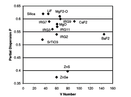
For secondary spectrum correction, the use of specific glass pairs such as BK7/SF2 or FK52/KZFS1 is effective. Implementing apochromat or superachromat lenses is advantageous for correcting chromatic aberrations across 3-4 wavelengths. During our research, we utilized Herzberger’s approach, which facilitates the selection of glass types for doublets and triplets by utilizing plots of partial dispersion versus Abbe number. This method significantly simplifies the process of choosing appropriate glass materials.
For NIR applications, combinations such as fused silica, BaF2, ZnSe, and LiF are suitable for crafting high-performance triplets. Research suggests that configurations such as triplet-doublet or triplet-triplet are optimal for creating faster optical systems. Additionally, triplets generally outperform doublets in apochromatic lens designs, offering superior image quality.
Figure 3.1 V# vs Partial Dispersion http://opticalengineering.spiedigitallibrary.org/
4 Specifications
The objective lens will meet the following specifications:
| Primary Specifications | ||
| Specification | Value | Unit |
| Numerical Aperture | 0.65 | — |
| Wavelength | 500 – 1000 | nm |
| Full Field | 0.05 | mm |
| Effective Focal Length | 6 | mm |
| Angle of Incidence and Refraction | ≤ 45 | Degrees |
| Performance Specifications | ||
| Specification | Value | Unit |
| Axial Color | < 1 | μm |
| Polychromatic Wavefront RMS at full field | < 0.023 | waves |
| Combined Coma P-V | < 5 | nm |
| Packaging Specifications | ||
| Specification | Value | Unit |
| Working Distance [As-built] | 5 | mm |
| First element vertex to Image Plane Distance | 70.1 | mm |
| Number of Elements | 11 | — |
| Additional Notes | |
| Specification | Note |
| Polychromatic Wavefront RMS | Calculated at 632 nm wavelength for all fields. Wavefront specification is at best composite focus for all fields. |
| Combined Coma P-V | Evaluated with Zernike Coefficients Z7/8 and Z14/15 |
5 Design Starting Point
To start our design, we completed a patent search for designs within our specification space. We narrowed our search by locating patent designs for microscope objectives that had long working distances as that is a primary specification that will determine many features of the lens.
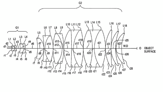
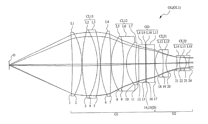
Figure 5.2 US Patent 10281703
With the patents, we take the lens prescriptions and import them into CODE V for further analysis. This initial evaluation focuses on lens performance, aberration balance, and material selection. After conducting an initial review, we begin the optimization phase. During this stage, we apply the various constraints to refine the patent design according to our specific requirements for the lens.
6 Intermediate Design
After optimizing the initial patent designs, we explored the design space with multiple variations, each dependent on the starting parameters. Most of these designs closely approach but do not fully meet the performance specifications. From these intermediate designs, we carefully selected a subset to further refine as we progress toward our final design. Below are a few examples of these intermediate designs.
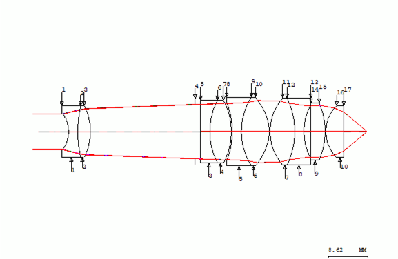
Figure 6.1 Intermediate Design 1
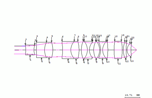
Figure 6.2 Intermediate Design 2
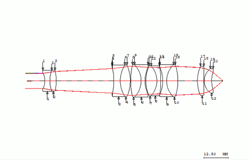
Figure 6.3 Intermediate Design 3
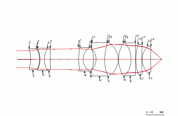
Figure 6.4 Intermediate Design 4
7 Final Design
Our final lens design comprises 11 elements, including three doublets, an aplanatic singlet group, and an air-spaced triplet, ensuring comprehensive correction across the lens system. With a NA of 0.65 and an EFL of 6 mm, this lens features a total optical path from the first vertex to the image plane of 70.1 mm, and a working distance of 5 mm, optimized for semiconductor applications. The design incorporates three elements made from low dispersion glass to effectively minimize chromatic aberrations. It achieves a nominal performance of 0.016 waves RMS at full field, within the customer’s specification of 0.023 waves RMS with a reference wavelength of 632 nm.
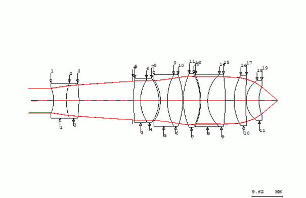
Figure 7.1 Final Lens Design
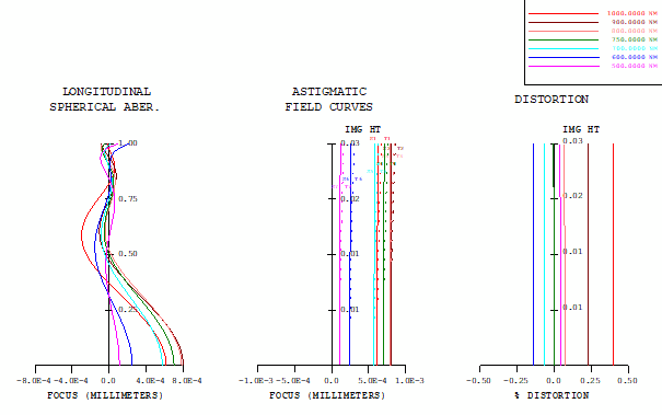
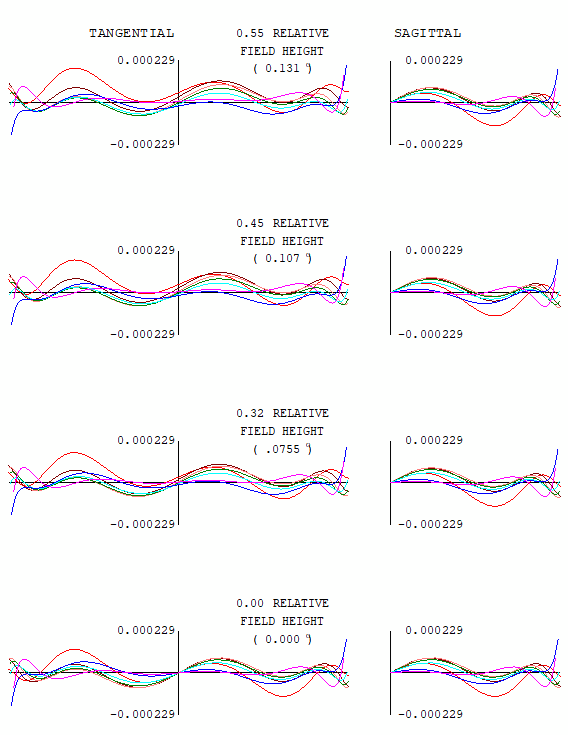
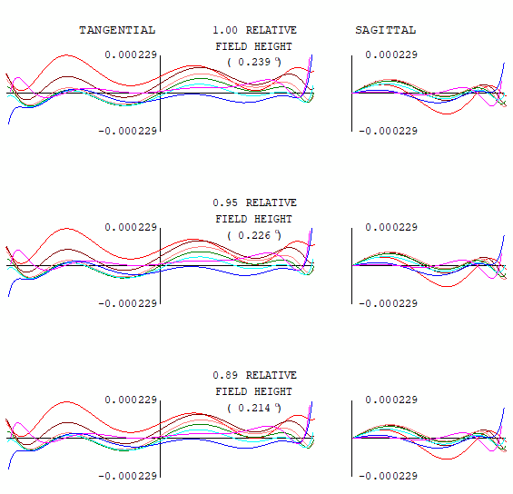
Figure 7.3.1 Transverse Ray Aberration Plot
The plots displayed here illustrate the wavefront RMS tolerance yield of this lens design. The yield for the full field at 0.023 waves RMS is approximately 67 percent, meeting our customer’s expectations. This design includes an image plane compensator, as well as airspace and lens element compensators.
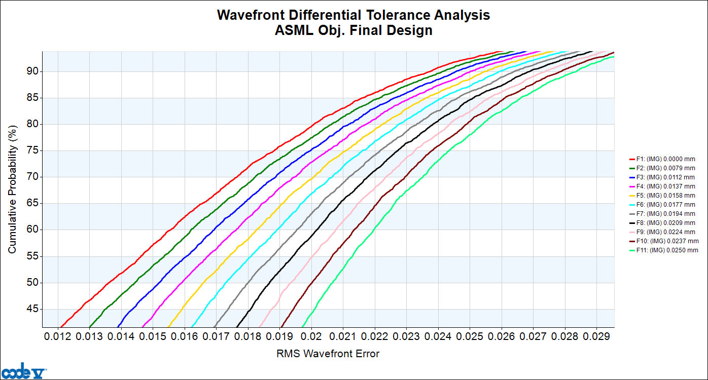
Figure 7.2 Final Design Tolerance Analysis
8 Conclusion
Our 11-element lens design meets our customer’s performance and tolerance specifications. Moving forward, we will continue to explore the solution space with the goal of further improving the tolerance yield. We appreciate this opportunity to contribute to ASML’s innovation in the semiconductor industry.
9 Acknowledgements and References
Acknowledgements: Thank you to Kirill Sobolev and Wayne Knox for their support and guidance throughout this project.
References:
[1] Taeko Toshi, 2019, MICROSCOPE OBJECTIVE LENS, US010281703B2. United States Patent and Trademark Office.
[2] Aligning Lithography to the Nanometer.” ASML, www.asml.com/en/news/stories/2021/fellow-simon-mathijssen-aligning-lithography-nanometer. Accessed 14 Dec. 2023.
[3] Ren, Deqing. “Apochromatic lenses for near-infrared astronomical instruments.” Optical Engineering, vol. 38, no. 3, 1 Mar. 1999, p. 537, https://doi.org/10.1117/1.602131.
[4] Development and Experimental Verification of an Analytic Model for Large Area Grating Couplers in Photonic Integrated Alignment Sensors, de Louw, N. 2022
[5] Schott AG (April 2005). TIE-29: Refractive Index and Dispersion. In Technical Information – Optics For Devices (Section 2.2). Retrieved from https://wp.optics.arizona.edu/optomech/wp-content/uploads/sites/53/2016/10/tie-29_refractive_index_v2_us.pdf
[6] Arisawa, K. (2000). U.S. Patent No. 6,016,226. Washington, DC: U.S. Patent and Trademark Office.