Team Members
- Yimin Chen
- Suheng Peng
- Xinyan (Cecile) Wang
Customer
- Andy Kurtz
- John Bowron
Faculty Advisor
Prof. Jaime Cardenas
Abstract
The camera system of Circle Optics is a 360-degree field-of-view stitching-free camera system used for small drones, entertainment, or robotics. The goal of our project is to create a hybrid optical design of the Circle Optics camera system including metalenses, glass, and plastic lenses. Metalenses are optical elements which utilize sub-wavelength features to manipulate the phase of incident light. These tiny features, called meta-atoms, are arranged in an array to optimize the wavefront.
Our approach is to explore the current advantages and limits of meta-optics with Meta-Optic Designer and PlanOpSim, and complete some meta-optics lab tests using a MoxTek metalens sample.
Design Methods

In this project, we are not responsible for the Opto-Mechanics and Sensor and Electronics of the system. The scope of this project is to focus on the lens system.
We utilized two softwares to design a hybrid design for Circle Optics’ camera system: MetaOptic Designer and PlanOpSim. Regarding to the first software, the way to approach this problem is to gradually create more and more complex problems for MetaOptic Designer to tackle, so we began with a hybrid Cooke Triplet design. With a hybrid Cooke Triplet design, we found out the capabilities and the limitations of the MetaOptic Designer. Then we moved onto the Circle Optics’ camera system, with one on-axis field and three wavelengths, we performed simulation and metalens design on replacing the telecentricity group and conic group separately. In parallel to MetaOptic Designer, we started PlanOpSim by taking out the last two elements and modeling the wavefront in Zernike Polynomials. We constructed a metalens that simulates the same phase and intensity profile as the replaced group over the same spectrum with a similar radius.
Simulation in MetaOptic Designer
In MetaOptic Designer, we created the Circle Optics’ camera system lens materials in the RSoft. Due to limitations of the MetaOptic Designer, we scaled the Effective Focal Length (EFL) of the Circle Optics camera system by a factor of 0.5 before we ran simulations. With on-axis field and visible spectrum, we first replaced the last air-spaced doublet in the telecentricity group. We tried three types of meta-atoms in the MOD database: hexagonal Si3N4, circular Si3N4, and square TiO2. Among three hybrid designs, the metalens uses hexagonal Si3N4 shown the best performance, with the on-axis MTF to be around 0.2 at 100 lp/mm for three wavelengths.
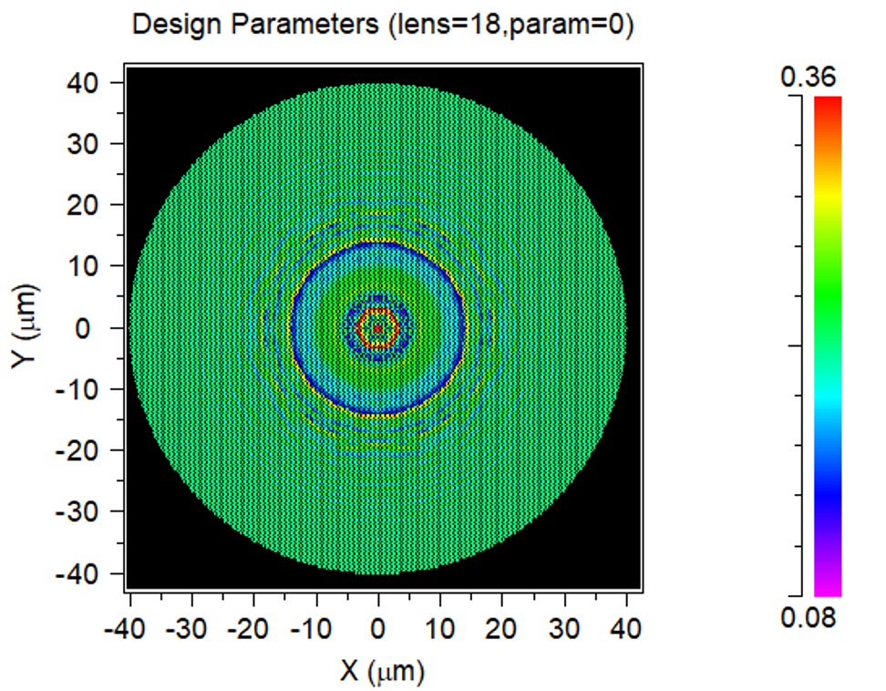
Then, we tried to replace lens 5 of the camera system, which includes an aspheric surface and a conic surface. We used a circle camera system which was scaled by a factor of 0.75. With on-axis field and visible spectrum, we found out that the results were not good unless we used the Si3N4 database. There are many more parameters that we could have varied.
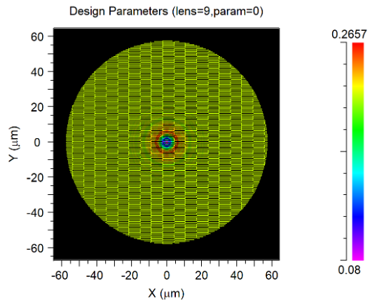

However, MTF curves generated by the MetaOptic Designer looks very unusual and shows a worse result compared to the original lens design. MetaOptic Designer is still a developing tool, with its own software related issues. This could explain the lower MTFs.
Simulation in PlanOpSim
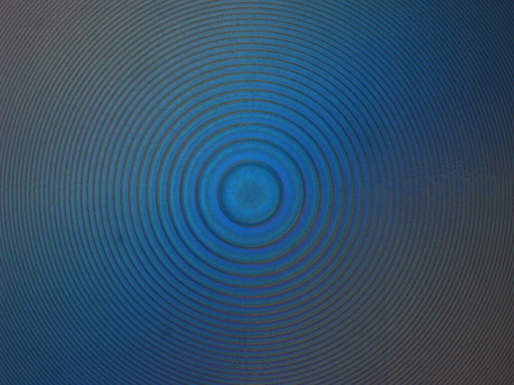
In PlanOpSim, based on the on-axis, visible-spectrum wavefront, shape, and radius of the last air-spaced doublet, we simulated a 4×4 mm metalens that generates the same wavefront information and phase information. This metalens consists of eight kinds of TiO2 circular pillars with different radii from 10 to 225 nm, with a transmission of 92%. The result phase profile is described in Cartesian Zernike Coefficients and simulated in a scaled-down version in PlanOpSim-based analysis. By zooming into the center of the metalens output, we can see some bullseye and crossed patterns in the picture, which indicates that this metalens should be working to achieve the wavefront pattern targets we set in the optimization process. Unfortunately, PlanOpSim does not have a built-in MTF like MetaOptic Designer. Performance analysis will require importing the metalens into CodeV or Zemax. Replacing two classic components that are used for telecentric purposes in this system with a metalens singlet is proven possible.

Metalens Sample Under Optical Microscope & Scanning Electron Microscope
Moxtek has provided the University with a metalens sample. The clear aperture of the metalens is 2 mm in diameter on 0.7 mm thick Eagle XG glass substrates. The lenses were designed for only 532 nm wavelength light. In addition, the sample has a focal length of 0.5 mm. These details can help orientate what kind of physical dimensions are realistically manufacturable.
Optical Microscope
When it comes to what we can test with the sample, we have several options. Firstly, we were given very little information on the metasurface atoms. It was valuable to inspect the metalens under an optical microscope.

Scanning Electron Microscope (SEM)
Scanning electron microscopy is an imaging technique which can easily image the meta atoms in the metalens. Scanning electron microscope relies on the sample being conductive for imaging. Unfortunately, the glass which makes up the metalens from MoxTek is not a conductive material. This means that we needed to gold sputter coat the sample before the SEM.
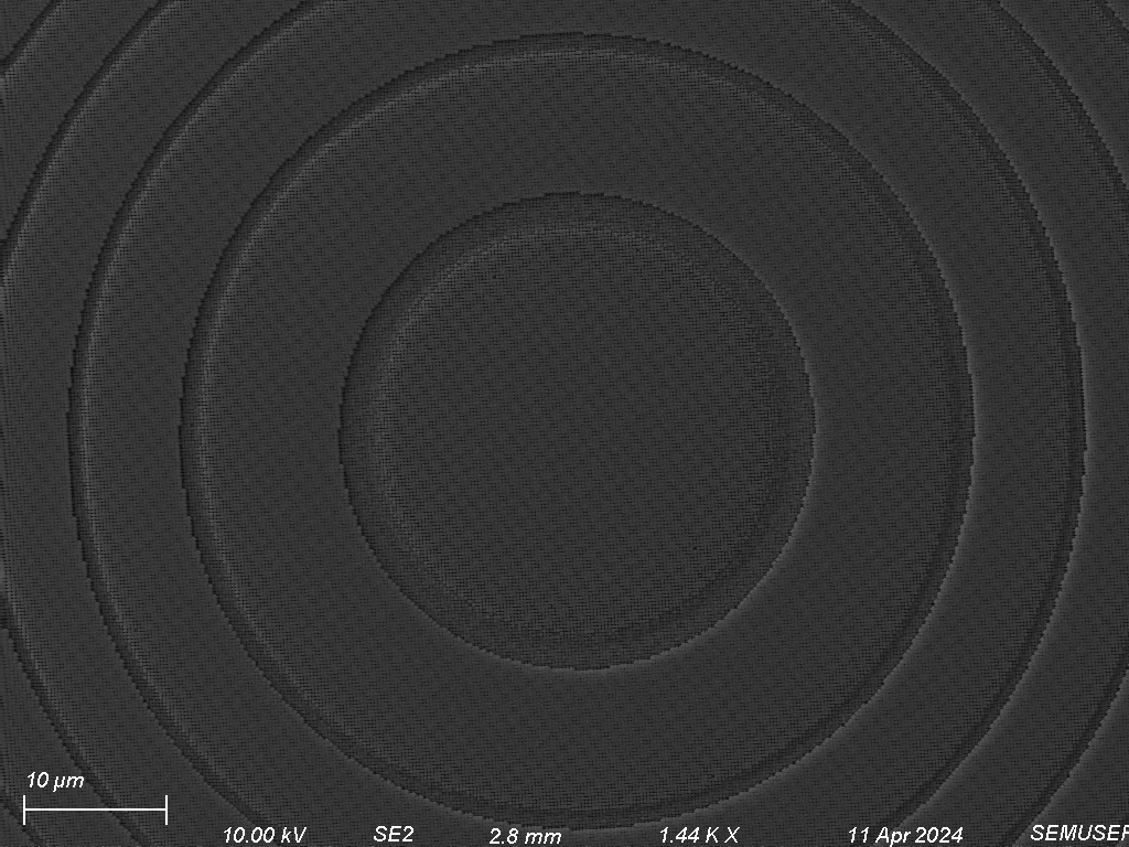
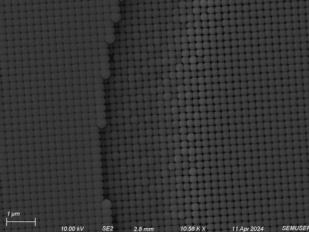
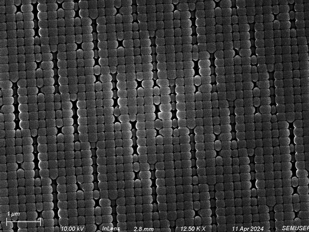
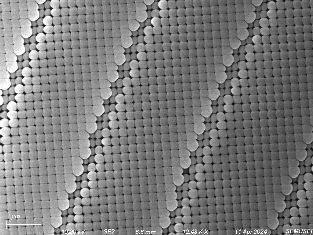
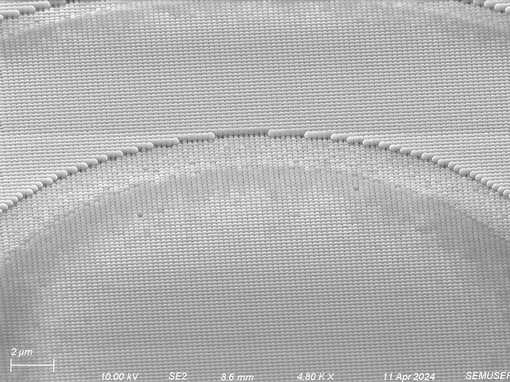
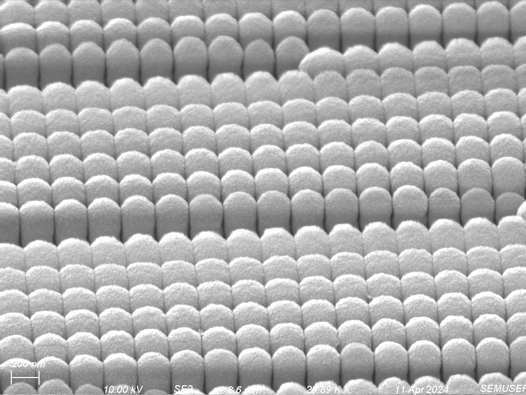
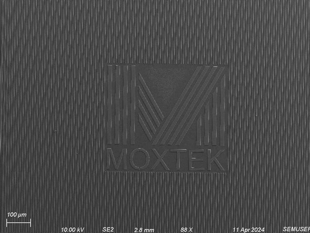
Images of the MoxTek sample under SEM
- Figure 1: Image of the very center of metalens. We can see a series of ringed valleys in the meta-atom structure. This means this sample has multiple layers of meta-atoms;
- Figure 2: Zoomed in image of one of the ridges at the center of the metalens;
- Figure 3: Image near the edge of the metalens. We can see that instead of rings, there are individual gaps in the meta-atom array;
- Figure 4: Zoomed in image of one of the ridges near the center of the metalens from the top down view;
- Figure 5: Zooming in more on the center, at an angle of 50 degrees. We can clearly see the ridge and the second layer of meta-atoms;
- Figure 6: Image of the ringed valleys at the same position as Figure 4, at an angle of 50 degrees;
- Figure 7: Moxtek logo on the metalens aperture under SEM.
Discussion
It was very difficult to design a hybrid system in MetaOptic Designer due to the computational limitations. We would expect the result is not accurate because the software could not perform simulation or analysis with the original lens size, but the meta-atom shape and material is chosen for future work. Considering the meta-atom pattern and arrangement we saw in the MoxTek metalens sample, the simulation result from PlanOpSim using wavefront construction is more promising.
To manufacture metalenses, the employment of nanostructure devices is essential. The main techniques available nowadays are E-beam lithography, DUV lithography, and nanoimprint lithography. While these methods are only good for printing complex patterns on a flat surface, they face limitations when it comes to varying the thickness of the lens.2 According to the MoxTek website, the sample we got was manufactured by using nanoimprint lithography. This method is known for its efficiency and precision in pattern replication. MoxTek further enhances the quality and consistency of their products by implementing the Statistical Process Control (SPC) monitoring of post-print Critical Dimension (CD) repeatability.3