Abstract
The aim of this project is to explore designs for a vibrometer for semiconductor wafer measuring machines. These wafers power all of our modern computers and cellphones, and are naturally in extremely high demand.
Currently, efforts to measure them are being hindered by vibrations – the system is moving at such a fast speed that the wafers are left vibrating during the measurement. This is where our project comes in: tracking the vibrations as the system is run will permit the measurements to be corrected, so that the measurement system can be run at faster speeds.
Team Members
- Megan Fallon
- Isabella Feraca
- Wutong Huang
- Geva Ozeri
Customer
Greg Jenkins – ASML
Faculty Advisor
James Zavislan
Vision
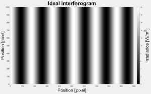
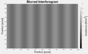
Our product is intended to work in conjunction with one of ASML’s wafer-measuring devices. This device utilizes point scanning at specific targets and a fast-moving table to scan the surface of the wafers to check for deformities. The vibrations of the table often interfere with the metrology and dilute precision and accuracy of the data. This manifests itself by washing out the visibility of fringes during image acquisition. Two sample interferograms show how washing out the fringes makes them far more difficult to read.
Unfortunately, taking more time between measurements will significantly reduce the output of the machines over time, so it is in our customer’s best interest to run the system at top speed and figure out how to correct the vibration issues. It has been determined by our customer that knowing the vibrations will allow their measured intensity to be corrected to its true value. Our job is to explore ideas for a device that can measure those vibrations. The device will be connected to the main sensor. The system would then measure only the relative vibrations between the sensor and the current wafer being measured on the translation stage.
Design Challenges
Because the vibrometer needs to measure on the order of fractions of a nanometer, just a simple interferometer will not do the trick.
Additionally, the team considered designs that could be mounted to the existing sensor, and focused on the same point of interest being measured by the main machine. This means that our vibrometer would have to operate from an oblique angle of incidence. However, the value of measuring the same point as the main sensor is that tilt and warping of the wafer table do not need to be factored into the design process.
Literature Search
The team performed a literature search, exploring the limits of a variety of optical sensing methods. The methods were compared to see which could best meet the specifications and geometry of the problem.
Some solutions explored include: laser doppler vibrometry (LDV), heterodyne interferometry, self-mixing interferometry (SMI), optical triangulation, Sagnac interferometry, CD reader technology, and laser speckle vibrometry. During our literature search, we were most concerned with systems that could handle our most limiting conditions: the ability to measure at a high angle of incidence, high resolution, and insensitivity to turbulence.
In addition to exploring solutions that would enable a custom system to be built, the team investigated commercially available systems to see what others in industry were able to accomplish.
Acknowledgements
Firstly, we want to thank our customer, Gregory Jenkins, for providing us with the opportunity to learn about and contribute to ASML’s amazing technology. We would also like to thank our advisor, James Zavislan for patiently guiding us through the process and ensuring that we learned throughout the whole project.